MADE BY:
Muhammad Inamullah (CEO)

Muhammad Mussab Bin Aamer (Wear house Manager)

Muhammad Shahab Ahmad (Marketing Manager)

Digital
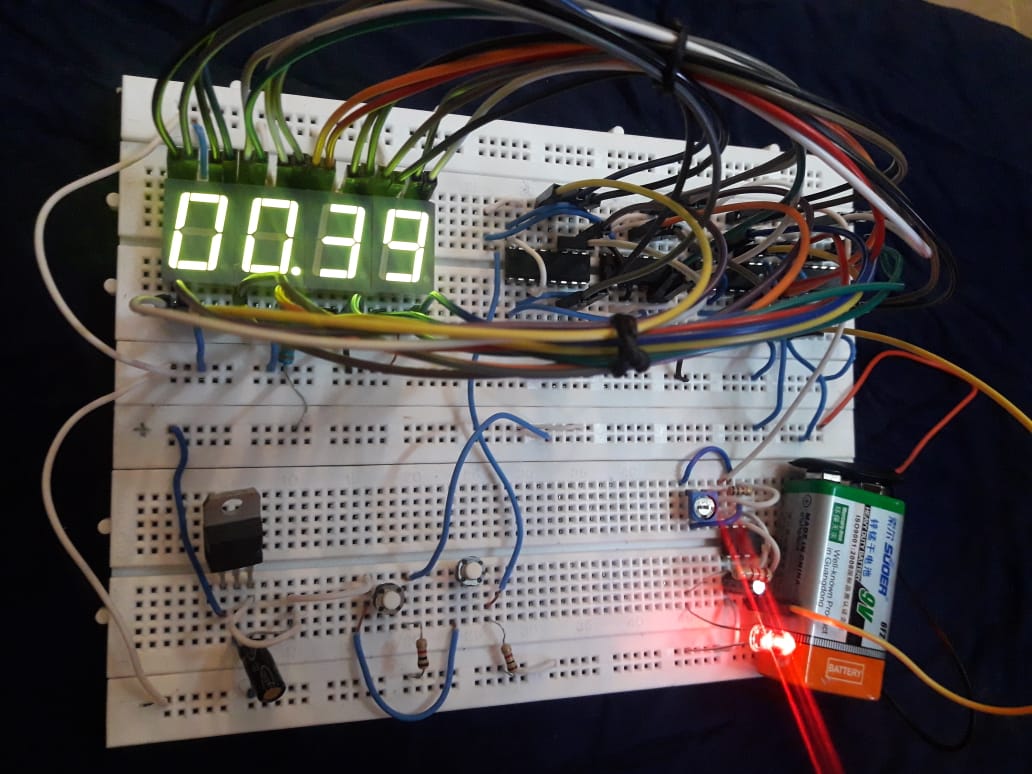
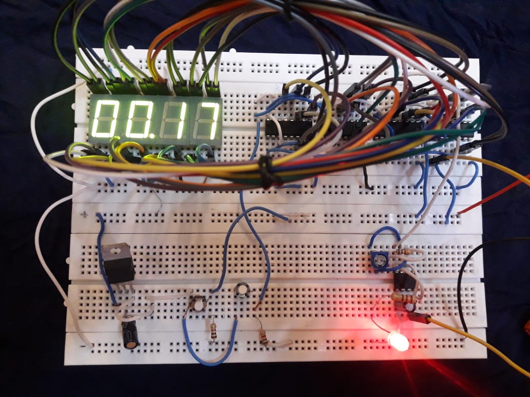
STOPWATCH:
Components:
- IC 4026 - 4
- 555 timer IC -1
- Common Cathode 7 Segment Display -4
- 150 Ohm -1
- 100K resistor -1
- 33K resistor -1
- 56K resistor -1
- 10uF capacitor -1
- On/off switch -1
- Push button -1
- Breadboard -1
- 9 Volt Battery -1
- Battery Connector -1
- LED -1
- Voltage Regulator 7805 -1
- Connecting wires
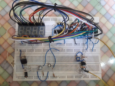
Digital Stopwatch Circuit Diagram and
Explanation:
In this circuit we
have used a 555 timer IC based a stable multi-vibrator which
is for creating 1-second delay. And two common cathode seven segment decoder
IC’s namely CD4033. The output of a stable multi-vibrator is directly applied
to seven segment decoder IC’s (U4) Clock pin (1) and carry output pin(5) of U4
IC is directly connected to the clock pin (1) of the second seven segment decoder(U3).
And two seven segments are connected with this decoder (U3 and U4). Its
connections are shown in the stopwatch circuit diagram given
below. One push button is used to stop /start the stopwatch and one push
button is used to reset the stopwatch. A 5-volt voltage regulator is used for
providing 5 volts to the whole circuit. And a 9-volt battery is used for powering
the circuit. Rest of connections are shown in the circuit diagram.

Working:
In this stopwatch
circuit, we have generated one-second delay by using 555 timers
based astable multi-vibrator. By using some calculation we can easily
generate a one-second delay. In a stable multi-vibrator, there are two resistors
and one capacitor is responsible for delay by charging or discharging the capacitor
through resistors.
We can set the 555 to work at the desired frequency by
selecting the right combination of resistances & capacitance.
Frequency = 1.44 / {(R1 + 2R2) * C1}
Also, 555 can produce waves with duty cycle else than the 50
% cycle.
Duty Cycle = (R1 + R2) * 100/ (R1 + 2R2)
where duty cycle = Ratio of the time period when the output is 1 to the time period when the output is 0.
where duty cycle = Ratio of the time period when the output is 1 to the time period when the output is 0.
In this project, we
have selects R1 is 1K, R2 is a 100K variable resistor and C1 is 10uF. [Also
check: 1
minute timer circuit]
As a stable
multi-vibrator generates one second's delay, this delay is oscillations or pulse
of 0 and 1. So we will use this pulse for triggering the seven segment decoder
then seven segment decoder changes the digit number with the one second of time
period.


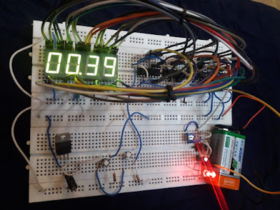
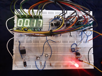
When we ON the
stopwatch (by start/stop button) it starts counting from zero and if we
turned OFF the same button then counting is stop or pause until again turned ON
the same button or press reset button.
There are four
seven segments, so this stopwatch
the circuit can count 00-59 seconds to 00-59 minutes time. Two seven segments
are for seconds and the other two seven segments
are for minutes.
Components descriptions:
IC 4026:
The IC
CD4026 is an IC which can perform the function of both a
counter as well a 7-segment Driver.
One single IC can be used to count from zero (0) to nine (9) directly on a
Common Cathode type 7-segment display. The count can be increased by simply
giving a high clock pulse; also more than one digit (0-9) can be created by
cascading more than one CD4026 IC. So
if you have a 7-segment (CC) display on which you have to display numbers that
are being counted based on some condition then this IC will be a perfect
choice.
How
to use a CD4026 IC


The 7-segment pins
will increment the count by one number each time when the clock pin (pin 1) is
made high. This clock source can either be obtained from a 555 IC or any other
digital IC which is TTL compatible. They simply have to generate a pulse of low
voltage 0V and high voltage 5V. In the circuit below I have used a clock source
of 1Hz to increment the count. So the number will get incremented for every
(T=1/F) 1 second.

The Reset pin (pin
15) is used to reset the count back to zero when made high. There are three
other output pins (pin 5,4,14) which will be used only when the IC needs to be
cascaded. The pin Carryover (CO – pin 5) will stay high by default, but when
the count reaches “9” it will give a small pulse and count will continue from
“0” again. This small pulse can be used to drive the clock pin of a
cascaded IC to display more than one digit. The Direct Enable output (DEO) pin
will always stay high, to enable any cascaded IC, if available. The Ungated C
segment pin (pin 14) is used for any division operation; this pin will stay
high by default and will go low when the count reaches “2”.

CD4026
Pin Configuration
Pin Number
|
Pen Name
|
Description
|
1
|
Clock (CLK)
|
The counting
happens when this clock pulse goes high, this pin is normally connected to
555 timer or other uC to produce a pulse
|
2
|
Clock Inhibit (INH)
|
Connected
to the Ground (low) of the circuit, to enable clock pin
|
3
|
Enable Input (DEI)
|
This
the pin is connected to +5V (high) to enable the output pins (Out A to Out G)
|
4
|
Enable Output (DEO)
|
This
is an output which always stays high, this pin will be only if more than one
CD4026 IC is used (cascaded)
|
5
|
Divide by 10 (CO)
|
This
is the carryover output pin; it produces a pulse after counting till 9. This
the pin will be only if more than one CD4026 IC is used (cascaded)
|
6,7,9,10,11,12,13
|
Out A,B,C,D,E, F,G
|
These
are the decoded output pins which should be connected to 7-Segment display.
|
8
|
Ground
|
The
the ground pin should be connected to the ground of the circuit
|
14
|
Not 2 out (UCS)
|
This
is Ungated C segment pin. This is an output pin which will be rarely used
when division is required.
|
15
|
Reset
|
This
input pin when made high (+5V) will reset the count to 0.
|
16
|
Vcc
|
This
pin powers the IC, typically +5V is used.
|
Features:
·
Counter for 7-Segment display
·
Can drive a common cathode 7-Segment display directly
·
Easy to interface with a timer or micron rollers (TTL
compatible)
·
Can be easily cascaded with more IC to display higher range
of number
·
Maximum Clock Frequency: 6Mhz
·
Available in 16-pin PDIP, GDIP, PDSO packages
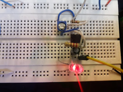
Clock
Source (multivibrator):

Individual Sequential Logic circuits can be used to build more complex
circuits such as Counters, Shift Registers, Latches or Memories, etc, but for
these types of circuits to operate in a "Sequential" way, they
require the addition of a clock pulse or timing signal to cause them to change
their state. Clock pulses are generally square-shaped waves that are produced
by a single pulse generator circuit such as a Multivibrator which oscillates
between a "HIGH" and a "LOW" state and generally has an
even 50% duty cycle, that is it has a 50% "ON" time and a 50%
"OFF" time. Sequential logic circuits that use the clock signal for
synchronization may also change their state on either the rising or falling
edge, or both of the actual clock signal. There are basically three types of
pulse generation circuits depending on the number of stable states,
• Astable - has NO stable
states but switches continuously between two states this action produces a
train of square wave pulses at a fixed frequency.
• Monostable - has only ONE
stable state and if triggered externally, it returns back to its first stable
state.
• Bistable - has TWO stable
states that produce a single pulse either positive or negative in value.
IC N555 Timer:


Pin diagram and description:
Some important features of the
555 timer:
555 timer is used in almost every electronic circuit today.
For a 555 timer working as a flip flop or as a
multi-vibrator, it has a particular set of configurations. Some of the major
features of the 555 timers would be,
·
It operates from a wide range of power ranging from +5 Volts
to +18 Volts supply voltage.
·
Sinking or sourcing 200 mA of load current.
·
The external components should be selected properly so that
the timing intervals can be made into several minutes along with the
frequencies exceeding several hundred kilohertz.
·
The output of a 555 timer can drive a transistor-transistor
logic (TTL) due to its high current output.
·
It has a temperature stability of 50 parts per million (ppm)
per degree Celsius change in temperature which is equivalent to 0.005 %/
°C.
·
The duty cycle of the timer is adjustable.
·
Also, the maximum power dissipation per package is 600 mW
and its trigger and reset inputs has logic compatibility.


Digital Stop Watch
555 Timer Generating Signal
No comments:
Post a Comment